The I/O devices are mapped in at
&A000
onwards.
VIA digital I/O &A000
The
6522 Versatile Interface Adapter is mapped in here; registers are as
follows:
&A000 IRB/ORB
&A001 IRA/ORA        ; with handshake
&A002 DDRB
&A003 DDRA
&A004 T1L-L / T1C-L  ; Timer 1
&A005 T1C-H          ; (is 16bit)
&A006 T1L-L
&A007 T1L-H
&A008 T2L-L / T2C-L  ; Timer 2
&A009 T2C-H
&A00A SR             ; Shift Register
&A00B ACR            ; Aux. Control Register
&A00C PCR            ; Peripheral Control Register
&A00D IFR            ; Interrupt Flag Register
&A00E IER            ; Interrupt Enable Register
&A00F IRA/ORA        ; no handshake
Please refer to a 6522 datasheet
for specifics.
ACIA
serial I/O &A100
The
6551 Asynchronous Communication Interface Adapter is mapped in here; registers are as
follows:
&A100 Transmit Register (Write) / Receive Register (Read)
&A101 Program Reset (Write) / Status Register (Read)
&A102 Command Register (Read and Write)
&A103 Control Register (Read and Write)
Please
refer to a 6522 datasheet for specifics.
UNUSED
&A200
This address is currently
unused
.
It could be utilised for an ADC or perhaps a second
VIA...
LATCH
&A300
The write-only
latch controls the four LEDs, assigned as
follows:
&A300 Bit 0 - RED LED
&A300 Bit 1 - YELLOW LED #1
&A300 Bit 2 - YELLOW LED #2
&A300 Bit 3 - GREEN LED
&A300 Bits 4 to 7 are unused
Expansion &A400+
Consider: Exchange the LATCH for a VIA. Drive the four LEDs
from the VIA. Add four more VIAs to the usused parts of the
address decode. This would give us ((8 x 2 x 6) - (4 + 2))
digital I/O lines, which is an astounding
ninety lines all individually
controllable; plus twenty four control lines which can be
interrupt-generating inputs.
Just imagine that in charge of a model
railway!
The memory decode
circuit decodes all eight I/O devices, but the
unused device select and the four
expansion device select signals are only available
from a connector that may be fitted as an option.
IIC
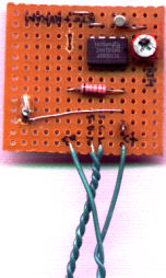
Basic support for the Philips IIC (or
I²C) protocol is provided from the uppermost two lines of VIA
port A. This is intended for use with a RTC/NVRAM circuit
(such as that pictured on the right), but it could be used for
other purposes such as teletext data acquisition.
The big open space on this circuit has
been provided for the inclusion of a rechargeable
battery.