Each part is discussed in further
detail within its respective sections.
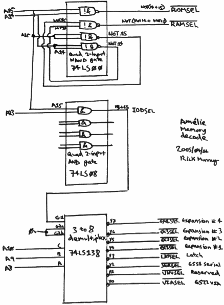
Address decoding (
first
attempt)
The
first
attempt at address decoding is as follows:

Click the
image to view a larger version...
This, unfortunately, has a giant flaw. Can
you spot it?
If not - consider that A14 and A15
both high mean the ROM is to be accessed; while A13 and
A15 both high means an I/O device is being
accessed.
However since
the ROM is mapped in at
&F000 , this in binary is %1111
0000 0000 0000; or in other words when accessing the ROM, A12,
A13, A14, and A15 will
always be
high. Thus, the I/O device selections will
always be active at the same time as
the ROM selection. Aaargh!
The solution is pretty simple and would
require only one more bit of logic to implement. But, it needs
NOT so this would be another logic gate. I
know I can do the entire memory
decode with three logic ICs (anything else is just
messy).
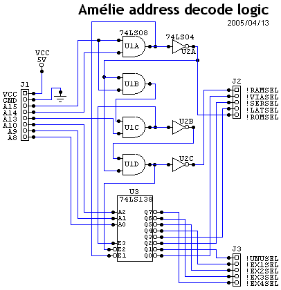
Address decoding (
second
attempt)
What was necessary was not, in fact, a
clever plot to fit in another logic gate; but rather a
complete rethink of the address selection logic.
I am not going to explain how I arrived at
the current decision, since the diagram pretty-much explains
itself.
Click the
image to view a larger version...
If you have ProTel's
CircuitMaker (or the
Pro version), or ExpressPCB's
ExpressSch and ExpressPCB (available from their website), you
can download schematics and circuit diagrams for
a hypothetical daughter-board to perform address
decodes.
This circuit will, however, be a part
of the main motherboard and not a
daughterboard...