Rick's b.log - 2017/05/12
You are 3.144.96.159, pleased to meet you!
Rick's b.log - 2017/05/12 |
|
| It is the 29th of April 2024 You are 3.144.96.159, pleased to meet you! |
|
mailto: blog -at- heyrick -dot- eu
Here are the DM320 GPIO assignments:
Neuros OSD test points
I had written most of this before I got ill. A brief tidy of the markup, and here it is... A list of the test points on the Neuros OSD board.
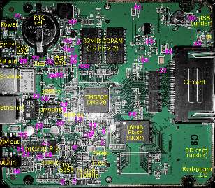
TP
Purpose
Expectations TP114.31818MHz clock to TVP5150 OSC
14.31818MHz waveform TP21.8V to TVP5150
+1.8V TP33.3V
+3.3V TP4+5V before YPS VREG
+5V TP5+3.3V after TPS VREG
+3.3V TP6Connected to GPIO1
? TP7SDRAM clock
SDRAM can clock up to 125MHz... TP8SD card DAT2
? TP9DM320 48MHz clock
48MHz waveform TP10PLL1705 27MHz clock
27MHz waveform TP11Audio clock
? TP1227MHz from PLL
27MHz waveform (for video encoder) TP13!RESET
High (+3.3V) unless reset TP14+3.3V to CF card
+3.3V TP15+3.3V pullup for CF control signals
+3.3V? TP16CF PWR ON signal
High (+3.3V) if CF powered TP17CF ENABLE
High (+3.3V) if CF enabled TP18DM9000 TXVDD
+3.3V? TP19DM9000 25MHz OSC
25MHz waveform TP20+3,3V for network interface
+3.3V TP21Right audio output
Line level audio TP22CVBS video output
PAL or NTSC composite video signal TP23Left audio output
Line level audio TP24Audio clock (at entry to CODEC)
? 27MHz? TP25+3.3V at OPA360 video filter
TP26Raw CV OUT (video prior to filter)
Akin to a composite video signal? TP27Filtered and shaped video signal
Composite video signal TP28Raw composite video input (or S-video luminance)
Composite video signal TP29Video enable, for switching composite video pass-through when powered down
+3.3V? to control relay TP30Power, +3.3V or from CR2032 cell, to MSP430 MCU
~3.3V TP3132.768kHz clock for RTC
32.768kHz waveform TP32MSPRST
Pulled low to reset MCU TP33IR IN
Raw signal from IR detector TP34IRQ from MCU
High if MSP430 wants to interrupt DM320 TP35IR Blaster
Signal from DM320 TP36IR IRQ
High if MSP430 wants to signal IR to DM320 TP3780kHz signal (from DM320)
80kHz waveform TP38Modulated IR waveform for blaster
Expect PCM at around 38kHz TP39USB PWR
High if USB port is powered TP40USB VBUS
+5V TP41+5V raw power input
+5V TP42+5V raw power input, after fuse
+5V TP43Master +3.3V after VREG
+3.3V TP44CVDD after VREG
? +3.3V? GPIO00 IN MSP430 IRQ
GPIO01 ? Pulled low, but has TP6
GPIO03 IN MSP430 IR IRQ
GPIO05 IN MS card detect
GPIO06 IN Ethernet IRQ
GPIO07 OUT USB power enable
GPIO08 IN SD card detect
GPIO09 IN CF card detect
GPIO10 OUT TVP5150 PDN (power down)
GPIO12 OUT PLL FS1
GPIO16 OUT LED red
GPIO17 OUT LED green
GPIO25 OUT CF enable
GPIO27 IN Serial RxD
GPIO28 OUT Serial TxD
GPIO29 OUT CF power enable
GPIO30 BI IIC clock
GPIO31 BI IIC data
GPIO32 OUT Enable video
GPIO33 OUT 80kHz
GPIO34 OUT Blaster signal (PWM)
GPIO35 IN SD write protect
GPIO36 OUT CF reset
GPIO37 OUT CF STSCHG
GPIO40 IN? TVP5150 C_WEN (active video area)
No comments yet...
| © 2017 Rick Murray |
This web page is licenced for your personal, private, non-commercial use only. No automated processing by advertising systems is permitted. RIPA notice: No consent is given for interception of page transmission. |